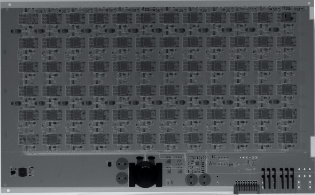
One of the challenging things with working on an L3+ hash board is the lack of a full set of schematics or gerber files available for the printed circuit board (PCB) to figure out the full function of the board. I’ve reached out many times to Bitmain but it’s not high on their list to release, guess they don’t want anyone reverse engineering the board…
Where does that put us, well, luckily the L3 has a huge community of folks constantly working on the hash boards and reverse engineering the board. RDC has done a great job of putting together schematics of some of the things the Bitmain manual lacks.
I also decided to dive a little deeper, with that I mean inside the board. I attempted to x-ray the PCB, hoping to gain a little more insight into the trace routing. The issue I ran into was the resolution of the x-ray and the energy put out was too high, washing a lot of it out. If that makes little to no sense, it’s like trying to watch an HD movie on an old tube TV. Regardless, some good came out of it and if you zoom into specific areas you can see some of the traces running to various points.

I built a high res video that shows the location of all components (and silkscreening on the board) for both the top and bottom. I will make the raw files available as well since it’s near impossible to find top side components without removing heatsinks. Luckily I have my practice board available…


