One of the challenging things with working on an L3+ hash board is the lack of a full set of schematics or gerber files available for the printed circuit board (PCB) to figure out the full function of the board. I’ve reached out many times to Bitmain but it’s not high on their list to release, guess they don’t want anyone reverse engineering the board…
Where does that put us, well, luckily the L3 has a huge community of folks constantly working on the hash boards and reverse engineering the board. RDC has done a great job of putting together schematics of some of the things the Bitmain manual lacks.
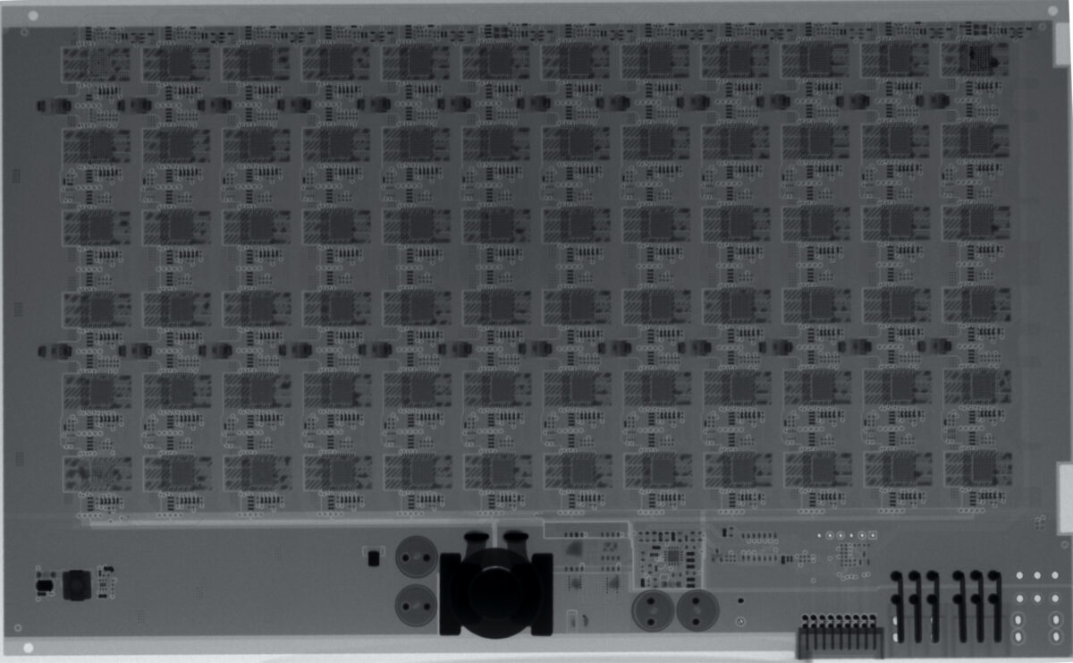
I also decided to dive a little deeper, with that I mean inside the board. I attempted to x-ray the PCB, hoping to gain a little more insight into the trace routing. The issue I ran into was the resolution of the x-ray and the energy put out was too high, washing a lot of it out. If that makes little to no sense, it’s like trying to watch an HD movie on an old tube TV. Regardless, some good came out of it and if you zoom into specific areas you can see some of the traces running to various points.
X-ray of L3+ Hash Board
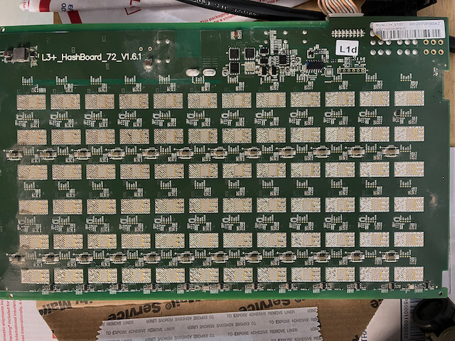
I built a high res video that shows the location of all components (and silkscreening on the board) for both the top and bottom. I will make the raw files available as well since it’s near impossible to find top side components without removing heatsinks. Luckily I have my practice board available…
Layer 1 of L3+ Hashboard PCB – Courtesy of RDCLayer 2 of L3+ Hashboard PCB – Courtesy of RDC
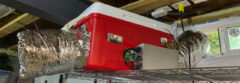
Like many of you I’ve had the displeasure of my L3+ lose a hash board, frustrating, but sometimes easily fixable.
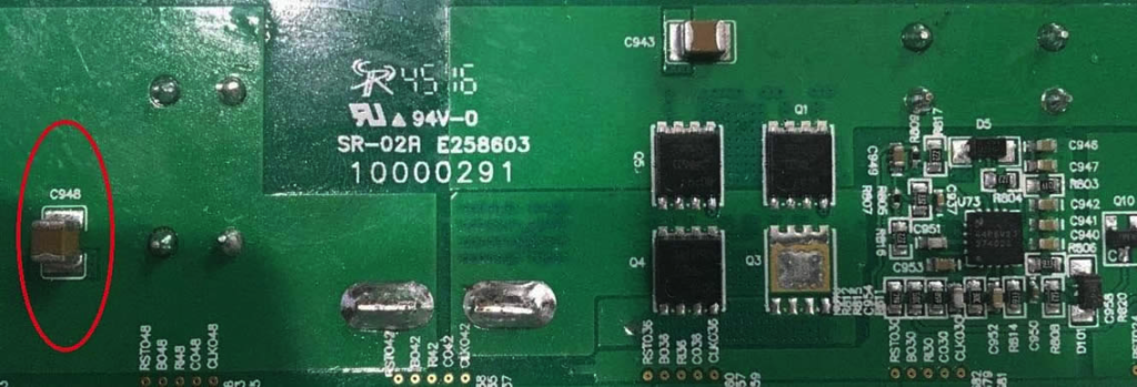
Often times, and I mean often, you’ll find that the 14.2V boost circuit has died which leads to your hash rate dropping to nothing for that board. I’ve seen many fixes (and attempts at fixes) and talked with a lot of folks about this. Some of the crazier things I’ve seen is removing C943 (still don’t know why they removed it) and running a jumper wire all the way across the board to D1. That gets you ~12V at the boost circuit (they did remove D1 to isolate from the old circuit) however that’s not enough to get the board to work to its full potential and it’s not a clean 12V so you can cause damage to your hash board down the line if you have power spikes.
NOTE – Per the manufacturer – Before applying power for the first time, turn the output voltage adjustment screw 20 full turns counter clockwise (CCW). Several people have reported the buck converter frying on the external module and this should insure it won’t burn out on power-on. Additionally insure you adjust the voltage using a multimeter before attaching the output to your hash board.
So I’ve had a hash board down for a few weeks and just now finally got a chance to take the unit down and see what we’ve got. Upon boot up the L3+ sometimes shows a missing hash board in HIVEOS (L3+_HashBoard_72_V1.6.1), as well as the stock firmware. Other times it comes up as anywhere from 2-72 chips (under ASIC status) found. I swapped cables and PS units and it still appears that way. Of note it also shows 0 for the PCB and chip temperatures, 0.00 for the MH/s (RT and avg), and strangely enough “Infinity” under W/MH.
December 1, 2021
I decided to start down the path of measuring various voltages and found the following after I inspected the 14V boost circuit (most common fault it seems:)
C1074 missing (no idea if it was ever there but the hash board did work fully at one point)
Voltage across C1072 – 11.98V
Voltage ground to L1 – 7V
Voltage across C1221 – 7.02V
So I started wondering if I’ve got a bad switching power supply in U111. I reached out to the Reddit world to see if anyone else experienced this on a hash board. I had a few folks reach out, but most the times it was to point me to the Bitmain L3+ repair guide (translated to EN.) This is a great general resource for L3+ troubleshooting, however it’s somewhat dated and really only deals with the V1.0 hash board which has different part numbering on the PCB and some completely different IC packages.
So time to get dirty again, I traced back to the DC/DC converter and found that there’s only a 7V output from there (which runs through L1), Q3/Q4 and across L2 only shows 6.94V so where do I go from here. I can’t find the V1.6.1 schematic anywhere online and can’t read the DC/DC part number to figure out what part it is. The PIC inputs are correct and it’s sending the keep alive every minute, so I think it’s somewhere between there and the boost circuit.
Update December 2, 2021
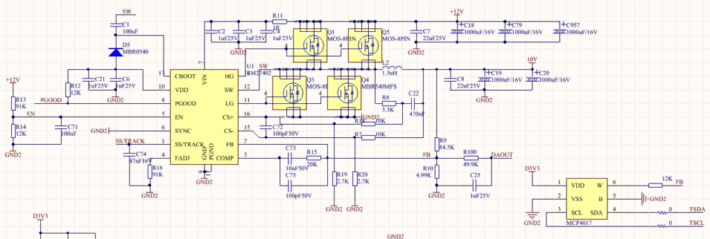
I think I have it narrowed down to before the boost circuit in the 10VDC rectifier. The big difference, other than the PCB numbering changing, is that the V1.6.1 uses a up9305W sync-rectified buck controller for the 10VDC and the older versions (1.5 and below) use the LM27402. Completely changes the circuit so the older schematics don’t help. Somehow either the up9305W is bad, or possibly a res or cap. I also verified the Schottky barrier rectifiers (MBR540MFS) on the output of the 10VDC circuit. Q1 and Q5 are tied between 12VDC and 10VDC (output) and Q3 and Q4 are tied between GND and 10VDC (output.) These then run through L2 before hitting the 14VDC boost circuit as well as other components.
Here’s a sample of what the circuit design should look like on the V1.6.1 version hash board, and the 10VDC should be generated by the internal Vref x (R1+R2)/R2.
(*From the data sheet) The output voltage can be programmed to any level between the reference voltage VREF up to the 90% of VIN supply. The lower limitation of output voltage is caused by the internal reference. The upper limitation of the output voltage is caused by the maximum available duty cycle (90% typical). This is to leave enough time for over current detection. Output voltage out of this range is not allowed. A voltage divider sets the output voltage (refer to theTypical Application Circuit on page 3 for detail). In real applications, choose R1 in 1kΩ ~ 10kΩ range and choose appropriate R2 according to the desired output voltage.
Update December 3, 2021
I decided to go ahead and install a new 14V boost circuit. This is an easy addition to the hash board, actually much simpler and cheaper than trying to replace the components on the board itself. It’s a relatively simple part to add, I used step-up boost converters I found on Amazon for just about $1 a piece.
When adding these in the key is to have a quality soldering iron as the temps needed to reflow the solder on the L2 lead is significant. Also insure you remove D1 so you isolate your new 14V boost circuit from the existing components and set Vout to 14V before soldering the wire to the D1 pad (you should solder to the D1 pad furthest away from L1.)
Now the big test, make sure you have both the power cables and comm cable to your control board attached as the processor is required to send the signal to the hash board to operate properly. Forget this step and you’ll just be chasing “ghosts in the computer.”
Did it work, well, yes now I measure 14V however that didn’t fix my hash board issue. Next step, well, I’m going back a step and will attempt to replace the sync-rectified buck controller to see if that’s causing the low voltage (7V) instead of the holy grail of 10V. It’s strange given all the faults on the board, but it’s a good next step given the fact that if the base core voltage is off, that can have a ripple effect across other components.
Update December 23, 2021
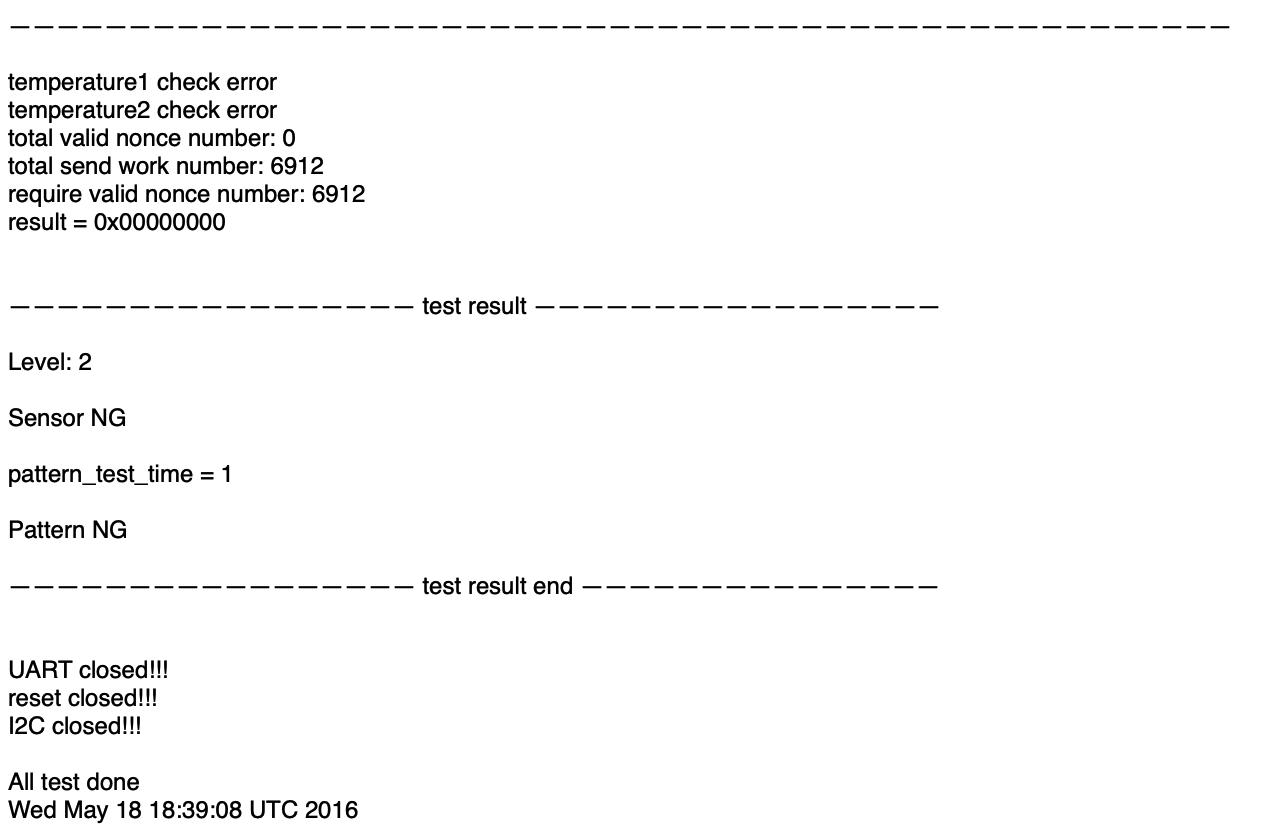
I put together a DIY test kit for the L3 and ran some diagnostics. It appears that my temperature sensor is most likely bad (flaky, which is bad.) So my next step is to replace that and see where that takes us!
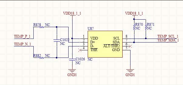
In reviewing the schematic of the temperature sensor, we can see that the TMP451 uses I2C to communicate on the hash board as well as having its own built in temperature sensor that is attached externally (pin 2 (D+) and pin 3 (D-)).
Credit – Bitmain L3+ Maintenance Guide
TEMP_P and TEMP_N are the PNP or NPN transistor in the ASIC (BM1485) itself that read the temperature. What I’m not sure of is which specific ASIC is it getting the temperature from as they operate in. I believe they use a thermal substrate transistor in one of the nearby BM1485 ASIC’s and have it wired to pin 6 (TEMP_N) and pin 7 (TEMP_P.) According the limited schematics I’ve seen they only show one representative sample of the BM1485 wiring and those pins are unconnected. I also see there are pads across the board for numerous TMP451’s, probably an enhanced feature they never implemented?
Luckily the TMP451 is in a WSON package, which makes it a complete pain to replace unless you have the right equipment and a steady hand. I suggest low temp solder paste in a syringe and a heat gun. I’ll try and video the process and post it when I’m done.
Update January 1, 2022
Finally success! I racked my brain for hours and finally decided that the buck controller wasn’t putting out the proper voltage. I inspected the PIC and since I could get some hashing I knew it was programmed properly, so I went back to PCB (printed circuit board) manufacturing 101, when it doesn’t work, rule #1 – reflow those solder joints.
I reflowed the PIC and the buck controller and viola! She’s hashing up a storm once again.
Reflow those joints, these circuit boards weren’t manufactured in the best possible environment
To continue our series on Bitmain’s Antminer L3+, we enter the troubleshooting phase. Over the last few months I’ve posted about various ways to extend the life of your miner and still maximize the efficiency. Well, sometimes we push a little too hard and see early failures and other times these units just get old and tired and start breaking. The question is what to do when it’s not doing what you think it should. Confusing? Don’t worry, I’ll walk you through creating a quick and easy (and cheap) way to test your L3+ hash boards.
I’ll start with saying Bitmain’s Support has been very helpful in getting me the firmware needed for this. There’s always going to be a slight language and time barrier, but they really did hook me up for this so I wanted to give them a big shout out. I haven’t been through their Antminer Maintenance Training Academy, which is generally a prerequisite for some of the support they gave me, but nonetheless they’ve really gone out of there way to help.
Bitmain created a maintenance firmware load that allows for running diagnostics on a unit without re-flashing the firmware that’s already flashed onboard the L3+ control module. This is exceptional for two reasons, one is obvious, we don’t have to re-flash and redo all our settings again. But two, we can test our units in place, and no special test fixture is required. It does help however to have a separate control board and I/O board for this, but it’s not required.
What you’ll need…
L3+ Control Board (I believe any version after 2.0)
Obviously you’ll also need some hash boards and a power supply, but that’s the whole point of building this so I’m guessing you’ve got those. I ultimately went the route of setting up a separate test fixture as I had the luxury of having a spare L3+ control board and I/O board.
Setting up the Diagnostic Firmware
You’ll need to get an SDCard that’s at least 8GB, clean and formatted FAT32 with only one partition for the entire device, and download the firmware here. The firmware image must be burned properly to the SDCard as there are several partitions that get created within the image. If you simply copy the image to a FAT32 formatted card you’ll be out of luck. I used the open source balenaEtcher which is a great free tool. Once installed, all you need to do is unzip the image to your hard drive theb open balenaEtcher. Once opened, it’s very simple:
And that’s it folks, a few minutes later you’ll have an SDCard that’s ready to roll and you’re already halfway there.
Setting up the L3+ control board for USB to TTL
Your next step is to add the USB to TTL adapter to your L3+ control board. This requires attaching three wires (TXD, RXD, and GND) to your control board. I highly recommend soldering the wires directly instead of the “cram and hold” method as that can lead to shorts and intermittent connectivity which will affect your results.
I used three male to female jumper wires for this as the female socket plugged directly onto the USB to TTL adapter and the male end fits into the L3+ control board sockets making for simple soldering.
For reference it will be easier to install the wires on the primary side (side that has the headers and most the larger components) of the L3+ control board and solder on the secondary side. There’s much more room to solder and less opportunity to damage anything. You just have to remember that you’ll need to bend the wires when you sandwich the I/O board on so plan for that when soldering (don’t mind the extra wires in the bottom right, that’s for another project involving an LCD.)
Attach power, USB cable, and computer
Once you have the control board and I/O board connected, attach the power header, your hash board to be tested on Chain 0 (I do one board at a time), and your USB cable to your computer. Open the terminal software on your computer and setup the USB serial port for 115200 baud rate, 8 bits, no parity, 1 stop bit, and RTS/CTS. Now select to connect (and if available select auto-reconnect as well.)
Insert the SDCard before powering up your unit and insure it’s inserted all the way by listening for the click that it snapped in fully.
Also if you’re running this outside of the chassis then insure you have fans cooling the hash boards or else you’ll create a whole new set of problems.
Now power on the unit and you should immediately be greeted by the following:
Once the system goes through its self-diagnostics it will enter a login screen, wait until it automatically logs in then you will reach the end of the boot up sequence when you see the following:
— get_works: wc_add_step = 1
At this point the system is ready to start testing any hash boards attached. In order to start the test you simply press the IP_Sig button on the L3+ I/O board. This will initiate a check for attached hash boards first, which is determined by the following:
As you can see from above, a value of “1” means the hash board is installed/recognized. The next steps simply read the hash board’s PIC, set the voltage, and set the frequency (stock 384MHz.)
After checking the hash board temperature the next step is running tests on individual chips (all 72.) I believe it accomplishes this by simply reading and writing to the memory. I believe the key thing here is that GAP_ERR, WORK_CRC_ERR, and CMD_CRC_ERR should all be “0” for each line.
After each ASIC has been tested the results will be published at the end:
Congratulations, you’ve run your first set of diagnostics on your hash boards and it should have only cost about $20 in parts and hopefully not too much labor. You will have to scroll through the terminal output to fully understand and appreciate what the test firmware is doing and understand a little bit about memory and registers, hexadecimal stuff, blah blah blah.
While this doesn’t point to anything directly at times, it can start to narrow down what you’re running into. I had one hash board that I believed the 14V boost circuit was bad on, turns out I had a bad temp sensor IC that intermittently read incorrectly so it was tough to track down.
Give it a shot and as always please give me feedback or experiences so I can improve this for others.
I’ve had a lot of folks hit me up with various overclock settings, and while most of them are within an acceptable range, there’s a few that really had me wondering when they would start seeing catastrophic failures. I consider this to be at a level where you far exceed the rated specifications of not only the unit as a whole, but even the individual components on the unit.
I’ll start with a disclaimer, actually more of a request, please don’t go crazy with overclocking until you understand the underlying negative effects and outright dangers. Any device you use to mine, whether it’s an ASIC or a GPU, has basic operating ranges and specifications for a reason, they’re safe, reliable, and repeatable. Once you step outside those limits you are literally taking a risk.
Update 12/27/21: I’ve had many folks ask how to measure their power draw. One solution that works very well is to install a Sense Energy Monitoron either your main electrical panel or a sub-panel that you have dedicated to your miners. This will give you real time feedback on the power (watts) used by your devices and make it easier come tax time to properly divide up your electrical bill and have the proof of the percentage you dedicate to your mining operation.
We’ll stick with the L3+ for this assessment, however many of the same lessons apply across all miners. Overclocking does more than just increasing your hash rate, to understand everything that’s going on we have to dive into some basic electrical principles.
Frequency (MHz not MH/s)
Frequency is basically the speed at which you’re operating the ASIC (MHz). Speed it up and you’re able to complete more “tasks/hashes” in a given period (time/seconds.) That comes with a cost, and that cost is paid for mainly in power and heat. To operate at a higher frequency than stock will require more power (watts), and with more power comes more heat. Yes, there are some variables like lowering voltage but you get the gist. So when you speed up your miner you draw more current, which increases your power, and generate more heat. Pretty simple, I’ll just speed up the fans and get a bigger power supply…
I’m pretty sure that’s what they thought too…
OHM’S LAW
We can go to an electrical staple to explain all of this, Ohm’s law: current (I) = voltage (V) / resistance (R). As you can see, there’s a direct relationship between these and power (W) as well. The Ohm’s law formula wheel is the best representation of the relationship between them all.
How this applies to mining is mainly covered the green (P) section. As you can see, power (P/watts) = voltage (V) x current (I). So when you crank up the frequency on your hash boards you’ll see the wattage go up. Ohm’s law tells us if you’re not manually adjusting the voltage, then you must be increasing the current.
Now let’s run some numbers based off some data I’ve collected in a past experiment. These are all straight frequency settings, at 9.92V, with no individual chip tuning.
Starting with the base L3+, running around 384MHz, you get around 203W per hash board. So 203W = 12V x (I)A, or 16.9A.
@448MHz we have 230W = 12V x (I)A, or 19.2A.
@472MHz we have 240W = 12V x (I)A, or 20A.
@490MHz we have 260W = 12V x (I)A, or 21.7A! (I’ll explain the exclamation below)
Note: There will be slight variations depending on the exact voltage settings you can use in certain firmware. For example, if you run the stock 384MHz but under-volt the boards (stock is 10.11V), you can safely run around 9.4V and you’ll consume less power.
So What, I have an 1800W power supply…
This is true, most power supplies have far more power than the unit requires. But just because you have it, doesn’t mean you should use it. Those little 6 pin connectors on the hash boards (2 per L3+ hash boards) carry a current rating anywhere from 8A to 10A, depending on the manufacturer and wire size. As you can see from the examples above, anything 240W and over you are most likely out of the operating range and that equals some excess heat, which leads to browning of the connector, and the higher/longer you go leads to deformation and failure (likely as a fire.)
Now let’s bring it all together. If we backwards plan our power consumption we see that we can’t support anything over 240W per hash board safely. There’s a key number to keep in mind when you’re tuning your miners. Why, for all the reasons above, we stay within specification of the main artery that runs the hash board. Burst that and you have catastrophic failure. So have at it, pump up that frequency, but when you do, keep the wattage under close inspection. You’ll have to drop the voltages down to keep it safe.
To continue the journey into setting up your crypto miners, specifically the L3+, you should start considering a long term electrical plan. What I mean by this is how can you optimize your existing electrical circuits in your home, office, shed, or wherever to gain the most MH/s(AVG) per watt (W/MH) and overall the most MH/s(AVG) per circuit.
Update 12/27/21: I’ve had many folks ask how to measure their power draw. One solution that works very well is to install a Sense Energy Monitor on either your main electrical panel or a sub-panel that you have dedicated to your miners. This will give you real time feedback on the power (watts) used by your devices and make it easier come tax time to properly divide up your electrical bill and have the proof of the percentage you dedicate to your mining operation.
I’ll assume that all units will operate off 240V for this, as it’s generally considered the most efficient as you pass less current through the wiring than you would if you went the 120V route, which minimizes cost and power transmission loss.
After some testing of various operating power/efficiency levels (Overclocking on the L3+, is the juice worth the squeeze?) of the L3+, I’ve got a good data set that gives me an efficient range to operate the L3+ within. So what now, data, great, how do I put it to use?
I ran the tests at frequencies from 384MHz (stock) to 500MHz and each frequency I ran at 9.5VDC, 9.8VDC, and 9.92VDC. The most ideal setting (with the best W/MH) for overall hashing rate was 469MHz, giving us ~608MH/s(AVG) @ 1.54W/MH (935W total.) The most ideal setting for overall efficiency (W/MH) was 384MHz, giving us ~504MH/s(AVG) @ 1.4W/MH (695W total.) A midrange that balances the two was 450MHz, giving us ~576MH/s(AVG) @ 1.52W/MH (873W total.) We also have to add in the wattage for the control board and fans. I took some measurements with an ammeter and found that the control board was only drawing about 10W and the fans, albeit variable, will generally draw no more than their max rating which would be ~30W each.
Note: These are all numbers that have not had any type of auto-tuning done at the individual chip level so your actual numbers can vary depending on that process if you chose to do it. These are just baseline numbers to go off of.
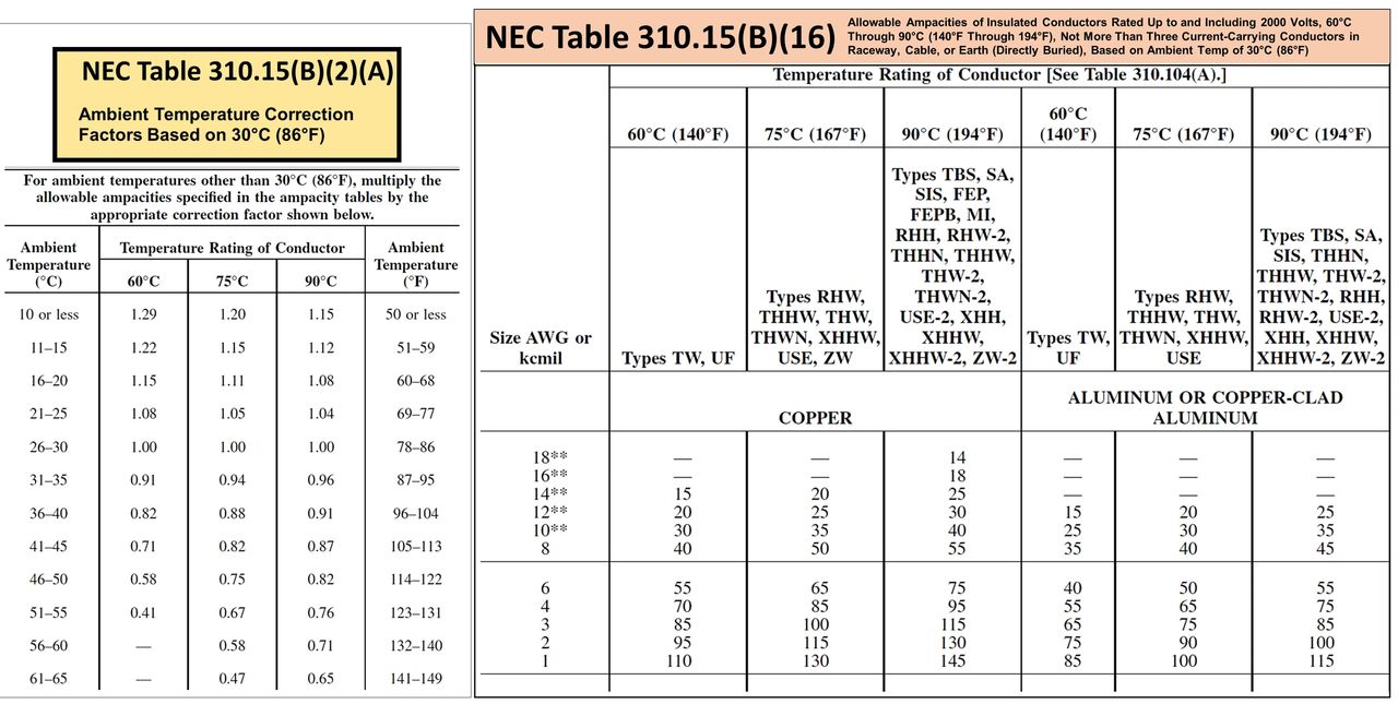
For those that aren’t familiar with residential or commercial wiring, a quick note on how much to load the circuits. The National Electric Code (NEC) essentially requires that each circuit have the ability to carry 125% of the continuous load. So if we have a 20A circuit, that is our theoretical 125%, which puts the continuous load at 16A (16A x 125% = 20A.) Head math shows that 16A is 80% of 20A, hence the 80% rule. After we determine the size of the circuit (i.e. 20A) we then reference the NEC code to find the appropriate wiring gauge for the circuit. This is code for one very good reason, you don’t want to overload and heat a smaller gauge wire too much or you’ll burn it up, and burn down your structure. I’m sure many folks have seen this on the DC side with wiring from power supplies to either ASIC miners or GPUs. I’ve chosen to use 20A for most my setups, mainly due to cost of the wire (12 gauge wire is significantly cheaper than 10 gauge), but also the efficiency calculations you’ll see later on in this post.
So let’s get into the meat and potatoes of what this is all about. I’ve listed out the most common circuits you’ll find and created scenarios based off those.
20A/240V – Given the 80% rule we have 3840W available to support our L3+ units.
3840W / 1005W = 3.82, so basically we can only run 3 L3+ units with plenty of room to spare and we are getting 1,824MH/s(AVG) out of the 20A circuit.
As a side note, we can toss one more L3+ in there at the most efficient setting (see below for wattage calculation) and that puts us at a total of 3780W and 2,328MH/s(AVG).
3840W / 765W = 5.02, so now we’re up to 5 units and we’re getting 2,520MH/s(AVG) out of the 20A circuit.
BALANCED
L3+ @ 450MHz = 873W + 10W (control board) + 60W (fans) = 943W total.3840W / 943W = 4.07, so now we’re at 4 units and we’re getting 2,304MH/s(AVG) out of the 20A circuit.
30A/240V – Given the 80% rule we have 5760W available to support our L3+ units.
5760W / 1005W = 5.73, so basically we can only run 5 L3+ units with plenty of room to spare and we are getting 3,040MH/s(AVG) out of the 30A circuit.
As a side note, we can toss one more L3+ in there at the most efficient setting and that puts us just over the 30A circuit at 5790W. Promise me you’ll unplug one intake fan (-30W) and that would give us 3,544MH/s(AVG).
5760W / 943W = 6.11, so now we’re at 6 units and we’re getting 3,456MH/s(AVG) out of the 30A circuit.
50A/240V – Did you disconnect your AC or hot tub for these miners or something?
You probably are spending more money in wiring (code says you’ll need 6 gauge wiring) then you can make on this circuit in a week. With the wiring and conduit, you’ll spend close to $5 per foot. In other words, stick with 20A (12 gauge wire) or 30A (10 gauge wire), the wiring is available at your local Lowes or Home Depot and comes in Romex so it’s an easier install without needing conduit. That’s all I have on this.
In summary, efficiency is king. Running out units at 384MHz and 9.5V yields us more than an 8% gain in MH/s(AVG) in a 20A circuit and a 14% gain in MH/s(AVG) in a 30A circuit.
Individual results may vary, take it for what it’s worth, but if you have the units, keep them running efficiently and you’ll get the most bang for your buck!
Like many of you I’ve often wondered just how much can I get out of my L3+/++, at just the level before I completely smoke it. For my own education I did some digging to find out just how much damage can be done at various overclocked frequencies.
Disclaimer – Every L3+/++ is different, every hash board is different, every environment we run these in is different, so these are just some baseline levels to consider.
Let’s just stick with the base L3+ set to the standard factory firmware and base settings. That puts us at an operating frequency of 384MHz and 10.11VDC per hash board IC (I’m using V1.5 hash boards.) That gives us our baseline of 504 MH/s (126 MH/s per hash board.)
Bitmain specs out the baseline L3+ at 800W nominal operating power, so if we take out ~60W for fans and control board, that leaves us with 740W total (185W per hash board.) Although after some research I believe they don’t account for the fans or control board on their specifications so let’s just set that number back to 200W per hash board.
Quick head math gives us roughly 1.59 W/MH, which is pretty much dead on from Bitmain’s specification of 1.6 W/MH. I ran one of my L3+ units at this level over the course of a few hours and saw that Temp(Chip) of each hash board remained at a very reasonable level, as shown in the chart below, but what’s interesting to see if the varying level of W/MH and Temp(Chip) levels throughout the experiment.
A few notes regarding the testing, I ran each speed/voltage for between 10-15 minutes as it takes about that long for the temperature and MH/s rate to stabilize. Additionally the ambient room temperature was 72 degrees and the fans ran at variable speeds, mostly between 5000-5400 RPM. Also a quick learning point for me, using ohms law we can see that each hash board requires approximately 17-20A of 12VDC.
The next three graphs show the three test voltage settings (9.5V, 9.8V, 9.92V) and the correlation of frequency (x axis) to MH/s(AVG) and W/MH (y axis.)
As you can see from the graphs, the actual (MH/s(AVG) is actual normalized rate which basically means this is the closest number to the actual work you’re doing. MH/s(RT) is an instantaneous value that doesn’t take Nonce% into account and can give you a false sense of the actual work you are doing. What does that mean, well as you’ll see in the next series of graphs, the AVG rate and RT rates track until we start getting massive amounts of HW errors which directly impact our Nonce%. For those that don’t know what the Nonce% is, it’s the ratio of HW errors to Nonce (numbers used only once.) The goal is to minimize the Nonce%, as well as the DiffA%. Generally if you’re not overclocking and un-volting too bad you’ll see a low number of HW errors which will keep your Nonce% under 0.03% (I’ve heard this arbitrary number many times and I still can’t explain it.) There is some direct correlation of the Nonce to the DiffA (difficultly of last accepted share), so keeping the Nonce under 0.03% keeps your DiffA near 0.0002% or less.
Long story short, if you hear about some amazing overclock settings where someone is getting 650-700 MH/s from an L3+, that’s most likely their RT and not the AVG, or actual work. I ran up to a 500MHz setting and got nearly 650 MH/s(RT), but as you can see in the data (and data doesn’t lie), the actual AVG rate was closer to 575 MH/s.
OK, great, thanks for all the data. So what does that mean for me, what are the best settings? I, nor anyone on the Internet, cannot answer that for you for the straight up reason that every board and situation is different. There are general guidelines to follow which I hoped to echo through this data. There is a point of diminishing returns, and that happens way before reaching temperatures that may damage your boards (generally under 75-80C.) A few graphs below show the varying temperatures and the slight rise with respect to operating frequency.
There are many different versions of firmware that can autotune, I actually use HiveOS on most of mine, and they do a pretty good job of fine tuning however you have to pick the basic frequency to run at before they can tune your L3+ in. If you are in a similar environment that I described then the data points to a sweet spot around 450MHz at 9.92V. That’s my basic starting point.
I hope this helps, and as always, hit me up with any questions or comments.
If you’ve heard it once, you’ve heard it a million times, you’ve got to keep the air cool and clean running into these L3+ units. In scouring the Internet I’ve seen anything from a class 1000 clean room to running big dryer sheets on the intake. I don’t really have the real estate or funding to put an ISO 9000 clean room in, conversely I’m not willing to risk the safety of my family and home to a dryer sheet being sucked in over the intake. The later of the two solutions being the cheapest of course, however the most risky since any restriction on the air intake can rocket the ASIC temperatures and cause an electrical fire that can have devastating effects beyond just the miner itself.
I’m all for minimizing the maintenance and increasing the longevity of my L3+ units, however this is really more of a hobby and not a full time job so finding the proper balance can be tough. I’ve talked to several people that religiously take their miners down on a monthly PM schedule, take the hash boards out, blow compressed air through them to root out any dust or contaminants (which having been in the circuit board manufacturing world in the past I can honestly say is a terrible idea, more on that later), and do the same for each power supply unit. What does that gain them, for starters they will collect less dust than someone that does that semi-annually or more, but how much dust really collects on the hash boards depends on your location.
Not my idea of inherently safe
I’ll be honest and upfront, I have run most my units for close to a year and other than an initial cleaning, I haven’t touched most of them since. That being said I’m not advocating that for everyone, in fact I was concerned with dust from where they are running as it’s an older warehouse, but they continue to crank along. I pulled one recently for a power supply cable issue (that’s another bloguverse entry) and went to inspect the hash boards and found very little dust, and no other contaminants to speak of. The only thing I can imagine is that the CFM of air moving across the hash boards, coupled with the fact that I cleaned them when I first got them, created a smoother surface where dust doesn’t settle. I have another unit I bought used from someone that obviously did oil immersion, that unit I could never quite get the hash boards completely clean and it picks up a tremendous amount of dust, so much that I do filter air for that one unit.
I learned early on, mainly through research but also through some practical testing on one unit, never restrict the intake airflow. How does one filter the air then, two thoughts come to mind, forced air or simply a larger intake that funnels down to the 120mm fan. I didn’t feel the need to invest in a forced air fan so I went with a system that uses a standard sized furnace filter and ducted that through two 4″ inputs that merge into one 4″ duct right at the 120mm fan. I used a 4″ duct shroud for the 120mm fan from Coolerguys.com and tied directly to my filter ducting.
After watching the L3+ status screen off and on for a few hours I saw no noticeable change in chip temps or fan speed. Is it a winner, sure, but when I put that side by side to all the other L3+ units I have I would say, depending on your situation, don’t get wrapped up in the idea you have to filter your incoming air. Definitely check your temps and fan speed daily, but absent any abnormalities, keep it cranking.